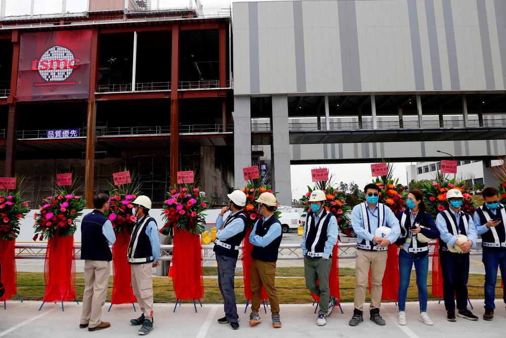
TAIPEI: Taiwan Semiconductor Manufacturing Co. (TSMC), the world’s largest contract chipmaker, touted its 3 nanometre process as the world’s most advanced semiconductor technology on Thursday at a ceremony announcing the start of mass production of chips using the highly anticipated technology.
The 3nm process yield rate is comparable to that of the 5nm technology and demand for 3nm chips are very strong, said TSMC Chairman Mark Liu during the ceremony held at TSMC’s Fab 18 in the Southern Taiwan Science Park in Tainan.
Liu said TSMC’s 3nm technology would feature an estimated 60 per cent gain in density of logic transistors and reduce power consumption by 30 per cent to 35 per cent at the same rate compared with 5nm technology reported CNA (Central News Agency).
Higher logic density means smaller transistors that operate faster and require less power to operate can be produced.
The 3nm technology can be used in cloud data centres, high-speed Internet, and many mobile devices, including augmented reality and virtual reality devices and demand for it is very strong, Liu noted.
After mass production of 3nm chips gets underway, the technology’s contribution to TSMC’s revenue is expected to be greater than that from 5nm chips in the same period, Liu said, adding that the mass production of 3nm chips will generate US$1.5 trillion in end product value within 5 years.
He said that TSMC’s Fab 18 had entered the eighth phase of expansion, which would make it twice the size of a regular semiconductor fab.
Fab 18 is an important production centre for TSMC’s production of 5nm and 3nm chips, and the total investment in the facility will reach NT$1.86 trillion (US$60.49 billion) and the investment is expected to create an estimated 11,300 direct high-tech jobs and 23,500 construction jobs, according to Liu.
Moreover, TSMC plans to recruit about 70,000 employees, he added.
Noting that TSMC will continue putting down roots in Taiwan, Liu said the company would officially open an R&D center in the Hsinchu Science Park in northern
Taiwan in the second quarter of next year and an estimated 8,000 R&D personnel would be stationed there.
He also said TSMC was planning to build a wafer fab using the 2nm process in Hsinchu and later expand production to Taichung in central Taiwan. - Bernama


